
SiliconIntervention is directly addressing the challenges of analog to information processing and compression identified by the Semiconductor Industry Association as part of the Decadal Plan.
SiliconIntervention has developed a disruptive approach to this problem over a period of several years. Now in place, this approach is actively giving rise to a series of real products that “answer the call.”
Lateral Thinking
While the digital designer enjoys the benefits of process scaling, his analog and mixed signal counterpart finds it increasingly difficult to create solutions for the analog signal processing chain. He can no longer accurately bias a device into an operating point with given gain or output impedance: all resistive, saturated and breakdown regions of a device become merged and very little “voltage space” remains to define accurate operation.
Some lateral thinking is needed.
Key to this thinking is to recognize that as process nodes scale there are also some significant features that create opportunities for the analog designer. Leveraging these features results in a set of “governing principles” which when incorporated within an agile development flow can be applied to multiple circuit designs and products. They enable us to solve the problem in a different way.
These governing principles together with a rich IP portfolio can be the data set for an agile mixed signal centric design tool suite. This has now been shown to be practical and fast and has produced results that answer the call for action.
Examples
A conceptual view of the development of a low power, data compressing ADC for ultrasound systems is shown below. For more detailed examples of our technology, see:
- The SI Neural ADC
- The SI Neural Network Analog FFT Computer
- The SI ANN exploiting Finite Rate of Innovation
- SI’s Neuromorphic Processing Circuits
- Signal Processing without kT/C Noise using Quantum Tunneling
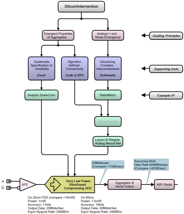
The approach relies on several component layers:
The First and Top Layer Comprises Guiding Principles (Pink)
These are used to underpin the design. They are fundamental techniques that can support a diverse set of circuit functions and implementations. In this example there are two:
The first guiding principle is one of Aggregation i.e. using the increasingly large number of minimum sized devices available to help solve the problem at hand. The subsequent steps in the development flow can rely on the aggregate behavior of many hundreds or thousands of devices in each signal processing step and benefit from the mean-of-means rule.
We identify two forms of aggregate behavior: static aggregate behavior and dynamic aggregate behavior. Static aggregate behavior is a means to make analog processing blocks like log convertors, multipliers, and envelope followers. These are very low power, and no clock is required.
Dynamic aggregate behavior is where the connectivity is varied with time, usually by a “one hot” signal that drives into the network from a delay locked loop or similar. Dynamic aggregate behavior is a means to make virtual oscillators, mixers, and filters etc.
A second is the guiding principle of Noise Emergence. This is the principle of processing the signal and its reference (its scale factor) concurrently in any bandwidth limited operation. This results in waiting, not for the “signal to settle,” but for the noise margin to reach acceptable limits. When we wait for the noise margin to emerge, we can pre-emphasize (prepare, or pre-set, give a hint to) the following circuits long before the equivalent settling time. This can be used to reduce power and improve performance.
The second layer comprises Development Toolset (Blue)
These tools efficiently use the principles to build, simulate, and verify the mathematical correctness of the design. They comprise an integrated platform that seamlessly connects sophisticated schematic capture, software defined functionality, and large math. spreadsheet analysis. They link to a traditional commercial set of simulation, layout, and other analytical tools.
Because the designs are based on potentially thousands of connected devices, we created a Schematic that has buses, iterated instances, and so forth. These are well-known and common to the first generation of tools that allowed analog designers to deal with complex circuits. But the Schematic adds to these features with table and code driven value variation with iteration index, variant iterated instance type (each repeated instances may look up its type in a data base), and code driven connectivity (the bus looks up or calls code to find its position in a higher-level bus).
Emergent behavior is supported by a systematic variation of either value, type, or connectivity vs position in a multi-dimensional array. To specify the incremental variation, we use Excel as the data source. Excel enables both a visual representation of the variability and arbitrarily complex relationships to be specified. Our tools interact with Excel ‘live’ through the Microsoft DDE/COM capability. The tools read and write into cells concurrently with user interaction.
Finally, there is one very powerful source of data that can control the instantiation of the many thousands of elements in these aggregate designs, and that is an industry known software algorithm.
For example, the Cooley-Tukey (CTFFT) recursive Radix-2 decimation in time algorithm is common in signal processing. Normally, the algorithm is given a data set and proceeds, through various recursive steps, to process the data into its Fourier domain representation. Thus, the algorithm has a control aspect (knowing what data item to operate upon at this step in the process) and an arithmetic aspect (knowing what operation to perform on that selected data).
SiliconIntervention takes algorithms such as CTFFT and transforms them such that the control aspect issues a netlist (a connectivity map), and the arithmetic aspect selects an electronic element for instantiation at that connectivity site. This results in a single call to the CTFFT creating a log-N deep, 2N tall neural network of fixed coefficients (the fixed “twiddle factors”).
This network has “unrolled” the recursive nature of the CTFFT and is an entirely analog device with 2N inputs and 2N outputs – the complex input and output of the FFT. Within a few nano seconds after the application of the analog input the analog FFT is available.
The described method is extended slightly in two ways: first the CTFFT is modified (as is well known in signal processing) to remove the redundant conjugate data of the “top half” of the output and so halve the size and power of any given network, and second the input is operated “round robin” allowing very high data sampling rates (>>1Ghz) and continuous FFT output. A proprietary SiliconIntervention algorithm (again a dynamic aggregate behavior device) removes bin-spreading in the rectangular round-robin sampler and provides exceptional signal fidelity in the output.
The FFT device is a remarkable example of dynamic aggregate behavior far exceeding the speed and power of a digital approach. It is supported by static dynamic behavior elements that take the logarithm of the output bin amplitudes and enable a second dynamic system to take the FFT of the FFT – so constructing a complete cepstrum analysis – the output of which is digital, easily matching customers’ expectations.
This we believe is the key to adoption of these ideas: all the IP augments the ADC conversion function. We move the boundary of the Analog to AI/DSP such that huge amounts of data compression and analysis are in the analog domain adjacent to the analog front end itself. This approach unburdens the AI/DSP from the common pre-processing tasks (such as FFT, Beamforming, time of flight analysis, MELS construction, and MFC encoding). These are done at lower power and much faster than the DSP can achieve and the data rate from these augmented sensors to the AI/DSP is far less.
The third layer comprises IP Portfolio (Green)
The tools link to a portfolio of analog and mixed signal IP, some of which are mentioned above. This is the third layer of the development stack. The guiding principles and supporting tools output these IP elements in industry standard form – it is the creation methodology that is novel and proprietary. The IP is verifiable in SPICE, mixed signal simulation and similar. The IP is delivered as documented GDS cells for incorporation into SOCs.
Extending the Landscape.
Scope
How can we extend the scope of this approach to other problems? (Not everyone wants to design an ultrasound compressing ADC shown in Part 1!)
Consider another example: an analog real-world sampler that inherently finds the Fourier transform of the signal. This has application in automotive (Lidar etc.), Medical (Pulse Oximeter) and AI / IoT (voice activity detect and voice recognition).
The ADC using this principle returns to the user not a sequence of time domain samples, but rather returns to the user the present value of phase and amplitude of defined FFT bins of the analog signal. In fact, that is what most of the voice processing applications do as a first step: the software converts the ADC time domain data into a perceptually uniform audio space (called the MELS space) and proceeds to find the cepstrum of the logarithm of these perceptually uniform bins. It then returns that spectrum of the spectrum. All those steps can be accomplished in the ADC using the SiliconIntervention methodology, and when we do this the power and the data rate from the ADC is much lower. (Interestingly, medical grade Pulse Oximeters do exactly the same thing – cepstrum of the log spectrum is processed.)
The methodology enables this innovation by allowing the engineer to explore a design paradigm where tens of thousands of analog elements exhibit an aggregate behavior to achieve, for example, the FFT and the log conversion.
How far can we extend the scope of this approach?
Extensions
We can extend the range of guiding principles. A third addition to the two shown in the example, is the principle of kT/C noise suppression. We turn a difficulty, namely growing gate current, into an advantage by modifying the input stage of advanced amplifiers to have a second servo mechanism around them causing the gate leakage current to cancel the kT/C noise – the input stage drives the output stage, but using the “free variable” of its output common mode voltage also drives a loop that manages kT/C noise. This can be exploited to vastly reduce power for a given noise.
We can extend the range of innovative IP to include many additional circuit designs. The development flow remains intact, is kept integral via the tools, and supported by any necessary process descriptions, industry standard simulation and layout tools
The development flow for several different target products is shown in the chart below, ranging from direct to FFT sampling through a fast ADC to an implicit logic family.
Development Methodology Examples Extensions

SUMMARY
- The number of real-world signals captured, and the digital information generated, vastly overwhelms our ability to process them efficiently
- Signal-to-data compression ratios demand orders of magnitude improvement in analog function performance and corresponding design methods to meet this challenge
- This demand is especially severe in battery operated systems
- Process scaling, driven by benefits to digital circuits, creates significant problems for analog designers
- An anisotropic view of process scaling reveals some guiding principles that have huge potential benefits
- These guiding principles can be efficiently incorporated into analog designs
- There are multiple guiding principles that have big impacts on signal-to-data compression
- A deep portfolio of ingenious inventions and know-how of analog circuit design are a necessary part of the solution
- A mature, agile, and easy to use development methodology that links all elements in the development flow has been put in place, while maintaining access to industry standard tools and design flows
- SiliconIntervention has put in place the elements to “answer the call”
- Multiple examples of end products using the development flow have been developed and are progressing through a silicon pipeline